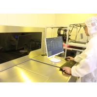
Product Description:
Laser Direct Imaging Printed Circuit Board (Laser Direct Imaging
Print Board, Laser Direct Imaging PCB) is a kind of PCB with
high-precision processing technology. It is characterized by its
effective exposure area of 620x720mm(24"x28.5"), file format
support for various formats, solder bridge/solder opening of
50/75μm(process Condition), line width tolerance of ±10%, and board
thickness of 0.5~3.5mm. It has excellent performance in terms of
accuracy, reliability and cost-effectiveness.
Features:
- Product Name: Laser Direct Imaging PCB
- Solder bridge/solder opening: 50/75μm(process Condition)
- Solder mask ink: 30s@600x500mm(24"×20")
- Alignment method: PAD(diameter: 0.5~3.0mm)
- File format: File Format
- Applicable process: Solder Mask, Outer
Technical Parameters:
| Parameter | Value |
|---|
| Line width tolerance | ±10% |
| Board thickness | 0.5~3.5mm |
| Solder mask ink | 30s@600x500mm (24"×20") |
| Solder Mask Color | Fixed Scale/ Auto Scale / Interval Scale / Partition Alignment |
| Laser power | Mixing Wave Total Power 512W |
| Alignment method | PAD (diameter: 0.5~3.0mm) |
| Application | PCB, HDI, FPC |
| Solder bridge/solder opening | 50/75μm (process Condition) |
| Effective exposure area | 620x720mm (24"x28.5") |
| File format | File Format |
Applications:
The GIS DPX820SM Laser Direct Imaging PCB is designed to be used in a wide range of applications. It is an
ideal choice for high-precision PCB, HDI and FPC printing. This
product has a high-precision PAD alignment method (diameter:
0.5~3.0mm) which ensures quick and accurate alignment. The
adjustable solder mask color includes fixed scale, auto scale,
interval scale and partition alignment. In addition, its board
thickness is 0.5~3.5mm, allowing it to be used in various projects.
This Laser Direct Imaging PCB offers superior performance with its
high-precision printing capabilities and reliable quality.
Customization:
GIS DPX820SM Laser Direct Imaging Printed Circuit Board
GIS DPX820SM Laser Direct Imaging Printed Circuit Board is a
precision laser direct imaging PCB with alignment accuracy of
±12um. It is applicable for Solder Mask and Outer Process. The
solder bridge/solder opening of this PCB is 50/75μm (process
condition). The effective exposure area of this board is 620x720mm
(24"x28.5"), making it suitable for PCB, HDI and FPC. This Laser
Direct Imaging Printed Board is made in Suzhou, China.
Packing and Shipping:
Packaging and Shipping for Laser Direct Imaging PCB
- The PCBs will be packaged in anti-static bags and placed in an
anti-static box.
- The box will be secured with bubble wrap and taped shut prior to
shipping.
- The PCBs will be shipped via a reputable courier service.
- The courier service will provide a tracking number to help monitor
the shipment.
FAQ:
- Q: What is Laser Direct Imaging PCB?
A: Laser Direct Imaging PCB is a high-efficiency production process
developed by GIS. It uses laser imaging technology to quickly and
accurately construct PCB patterns without the use of any
phototooling, making it a cost-effective and reliable option for
PCB production. - Q: What's the brand name and model number of the product?
A: The brand name is GIS and the model number is DPX820SM. - Q: Where is the product manufactured?
A: The product is manufactured in Suzhou, China. - Q: What benefits does Laser Direct Imaging PCB offer?
A: Laser Direct Imaging PCB offers many benefits, such as fast and
accurate PCB pattern production, improved quality of PCBs, and
reduced costs. - Q: What materials can Laser Direct Imaging PCB process?
A: Laser Direct Imaging PCB can process many materials, including
FR4, polyimide, aluminum, and copper.


