Sign In | Join Free | My himfr.com
Home > LDI Laser Direct Imaging >

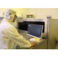
CE 610mmx710mm LDI Laser Direct Imaging Machine PCB

Jiangsu GIS Laser Technologies Inc.,
Trust Seal
Verified Supplier
Credit Check
Supplier Assessment
Contact Now
    Buy cheap CE 610mmx710mm LDI Laser Direct Imaging Machine PCB from wholesalers
     
    Buy cheap CE 610mmx710mm LDI Laser Direct Imaging Machine PCB from wholesalers
    • Buy cheap CE 610mmx710mm LDI Laser Direct Imaging Machine PCB from wholesalers

    CE 610mmx710mm LDI Laser Direct Imaging Machine PCB

    Ask Lasest Price
    Brand Name : GIS
    Model Number : DPX230
    Certification : ISO 9001 CE
    Price : negotiable price
    Supply Ability : 30set per month
    Delivery Time : 20 work days
    • Product Details
    • Company Profile

    CE 610mmx710mm LDI Laser Direct Imaging Machine PCB

    laser direct imaging (LDI) system solutions for various PCB Multilayer


    When Opt to LDI Technology?


    Existing technologies are unable to offer acceptable solution and the inevitable results is reduced PCB production efficiency and lower yields. Nowadays, an average PCB trace width reaches 0.075mm (3mil) in complex multilayer PCBs. While photolithography imaging process unfortunately reached its limits due to creating high density interconnects on PCB. It is unable to creating PCB below 0.127/0.127mm (5/5mil) of trace widths and spaces. So, when most of the trace widths and spaces on a circuit board are smaller than 0.127/0.127mm (5/5mil), LDI is the best imaging option.


    LDI technology is mainly used in HDI board manufacturing before. But now PCB manufacturers have to manufacture fine-line and ultra-fine-line conventional rigid, flex and rigid-flex PCBs with LDI technology where the trace widths and spaces of the conductive circuits are 0.075/0.075mm (3/3mil) or even 0.05/0.05mm (2/2mil). That’s because Laser Direct Imaging (LDI) has proved itself as the best and most comprehensive imaging solution for fine trace widths and spaces.


    How does laser direct imaging ( LDI ) work?
    Laser direct imaging needs a PCB with the photo-sensitive surface that is positioned under a computer controlled laser. And then the computer is creating the image on the board with the light of laser. A computer scans the board surface into a raster image, matching the raster image to a pre-loaded CAD or CAM design file that includes the specifications for the necessary image intended for the board, the laser is used for directly creating the image on the board.


    Specification/modelDPX230
    ApplicationPCB,HDI,FPC (inner layer,outer layer,anti-welding)
    Resolution (mass production)30um
    Capacity30-40S@18"*24"
    Exposure Size610*710mm
    Panel thickness0.05mm-3.5mm
    Alignment ModeUV-Mark
    Alignment capabilityOuter layer±12um;Inner laye±24um
    Line width tolerance±10%
    Deviation increase and decrease modeFixed increase and contraction, automatic increase and contraction, interval increase and contraction, partition alignment
    Laser typeLD Laser,405±5nm
    File formatGerber 274X;ODB++
    Power380V three-phase alternating current, 6.4kW,50HZ, voltage fluctuation range + 7% ~-10%
    ConditionYellow light room; Temperature 22°C ± 1°C; Humidity 50% ± 5%; Cleanliness level 10000 and above;
    Vibration requirements to avoid violent vibration near the equipment


    About us
    We are an innovative supplier of various PCB laser direct imaging (LDI) system solutions. Our system product portfolio ranges from LDI system configurations for high-mix and emerging PCB niche applications to fully automated LDI system solutions for mass production environments.

    Quality CE 610mmx710mm LDI Laser Direct Imaging Machine PCB for sale
    Inquiry Cart 0
    Send your message to this supplier
     
    *From:
    *To: Jiangsu GIS Laser Technologies Inc.,
    *Subject:
    *Message:
    Characters Remaining: (0/3000)